Traditional PICs (photonic integrated circuits) inherit the mature CMOS fabrication process from the electronic integrated circuit industry. But this process limits the PIC structure to a single waveguide layer. A research team from the Integrated Nano Optoelectronics Laboratory at the University of Michigan in Dearborn and the Energy Institute at the University of Michigan in Ann Arbor have explored the possibility of PICs with multiple waveguide layers. The team has developed a prototype of a true 3D OPA (optical phased array) device, with the light exiting from the edge of the device, based on a multilayer Si3N4/SiO2 platform technology. The pictures show schematically the construction of the device.
An optical fiber couples light into the device (picture A) and the waveguide width at the coupling region is enlarged to ensure the best mode matching (picture A1). A 2D, 8 × 16 OPA is formed at the edge of the device as an outcoupling unit (picture A2).
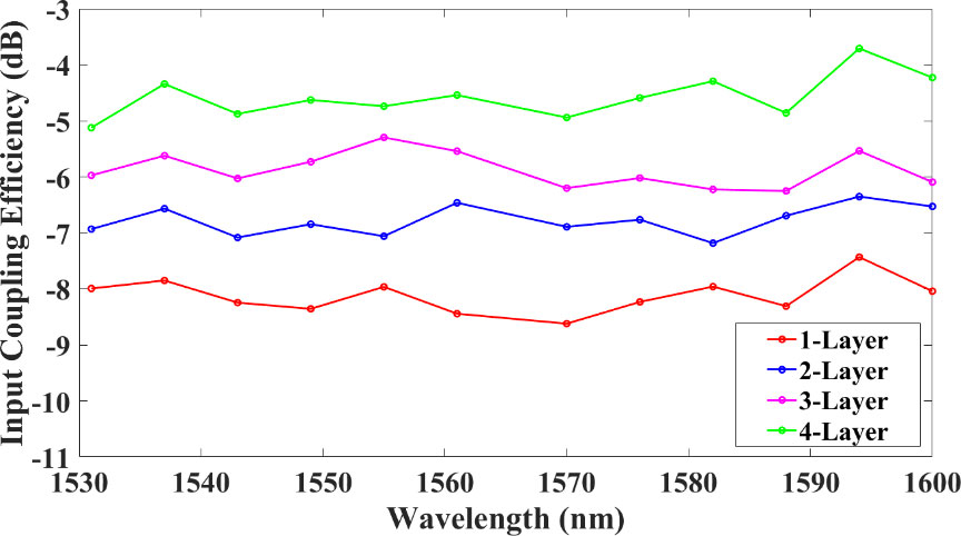
The multi-waveguide-layer configuration offers the possibility of using edge couplers at both the input and the emitting ends, to achieve broadband high efficiency. The team has studied the new concept by numerical simulation as well as measurements of proof-of-concept samples with one to four waveguide layers.
Typical measurement results for the Input coupling efficiency are shown in the diagram.

These encouraging results confirm the expectation that with multiple waveguide layers the coupling efficiency can be significantly improved.
According to the research team, this is the first experimental proof-of-concept of a true 3D OPA with multiple waveguide layers and compatible with CMOS manufacturing technology.
DVN comment
This research is another interesting contribution pushing OPA development. Though OPA is still in an embryonic phase, research departments of industry lidar suppliers should keep a close eye on this technology. DVN will regularly keep you updated on our observations in this technology segment.
